

Neurotech student clubs and researchers wanted to investigate the neuron’s response to nootropics, sleep peptides, capsaicin, or mushrooms’ abilities to use language. However, the component which interfaces with the neurons—microelectrode array—tends to have long-shipping times and also costs $300. It just is a miniscule grid of wires! So, we’re building a cheap MEA, and so far graphene version costs <1$ and 5.5 min per unit.
Quick glance of methods we’re testing
Laser deposition of metals
Laser-induced graphene
Aluminum vapour deposition
Copper metalization
Laser ablation
Indium tin oxide
Design files
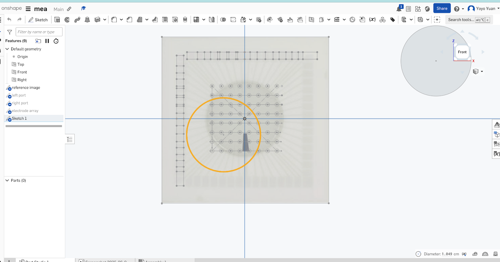
Designing the initial MEA in onshape:
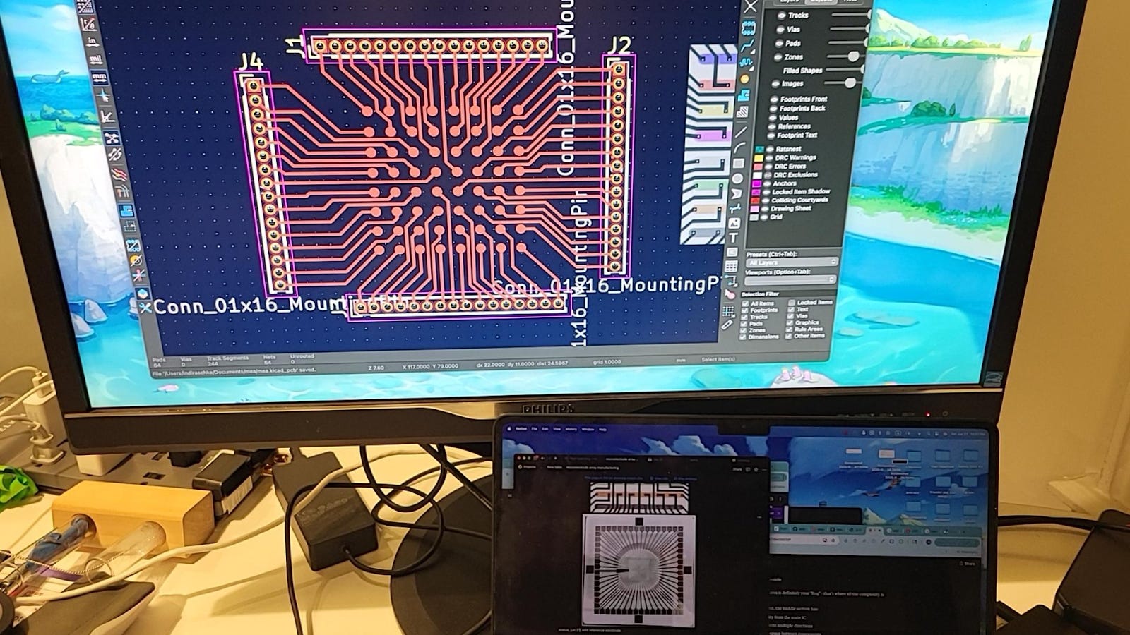
The improved MEA in KiCad.
Essentially, the dot grid directly come into contact with neurons, and extend out to the peripherals. I made a mistake at first to draw the ring too conductively, which would undesirably connect all the electrodes together.
Laser-induced graphene
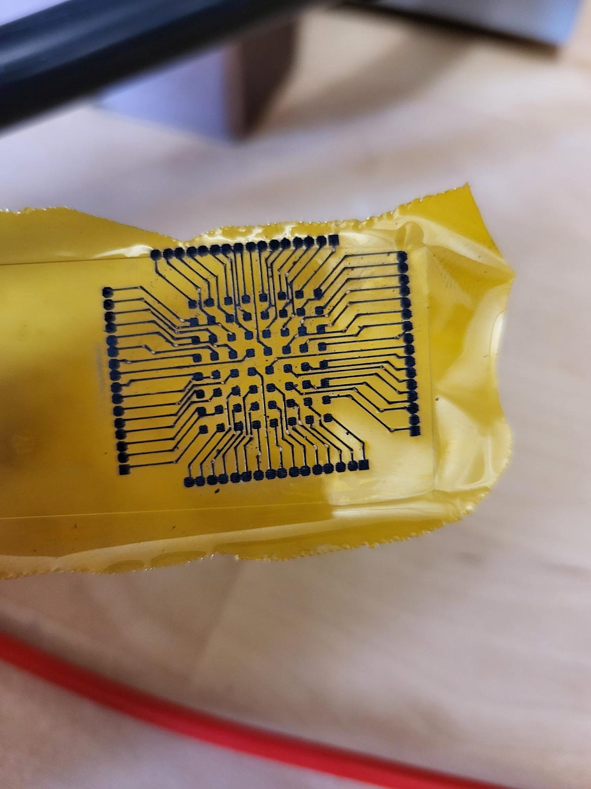
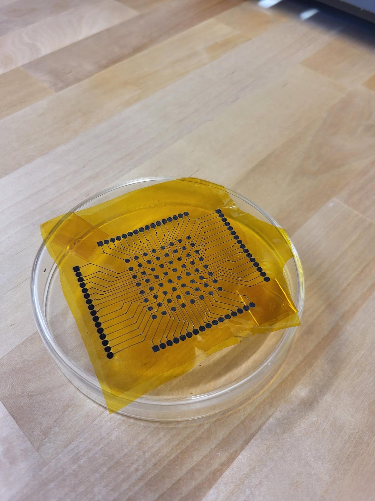
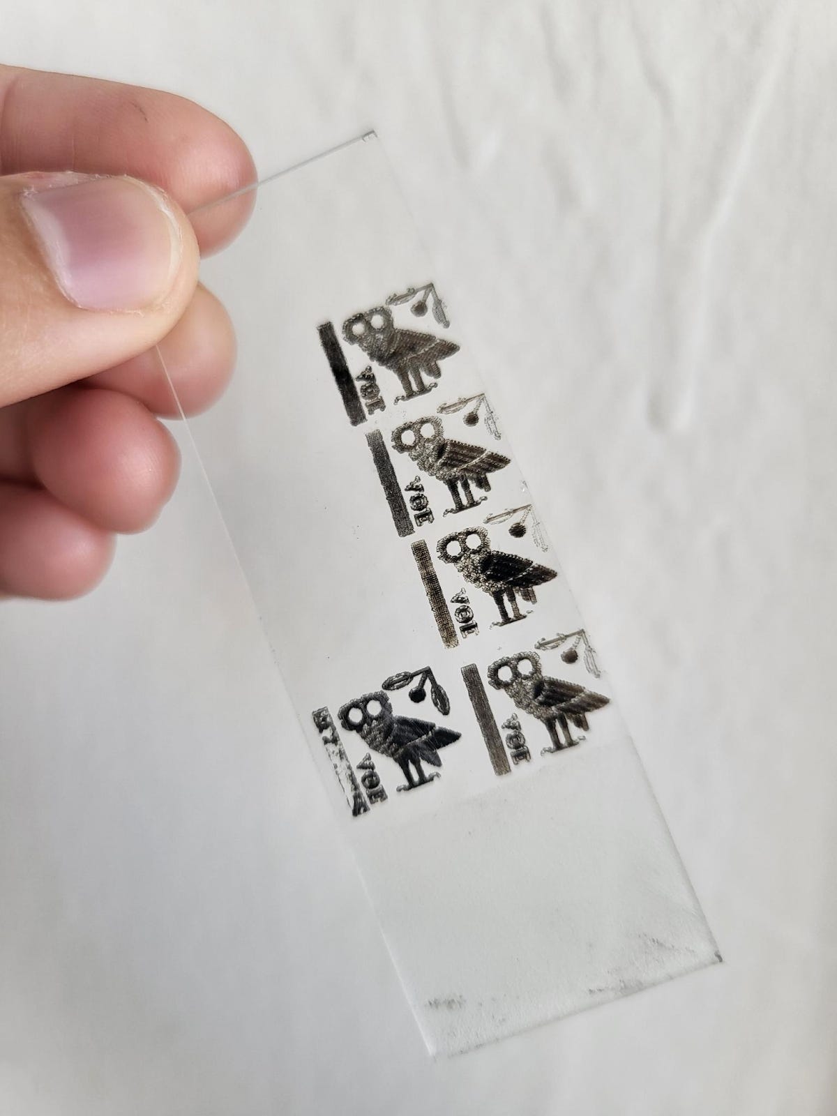
We direct a laser at this yellow tape, for graphene to become deposited on the surface.
Using a CO2 laser of 10 600 nm with 5.5W at the scanning rate of 88 mm/s with 100 lines/cm (paper), we shined a beam through kapton tape. Kapton is an insulating tape made of polyimide. The laser’s energy causes lattice vibrations, creating high surface temperatures of possibly >2 500 °C. Under the high temperature, C=O, C–N, and C–O bonds are broken, releasing the non-carbon gases. The carbon atoms rearrange into graphene with its hexagonal structure.
The centre-to-centre distance between electrodes: 0.15 cm, with a 0.25 cm electrode radius. The trace width: 0.2 mm.
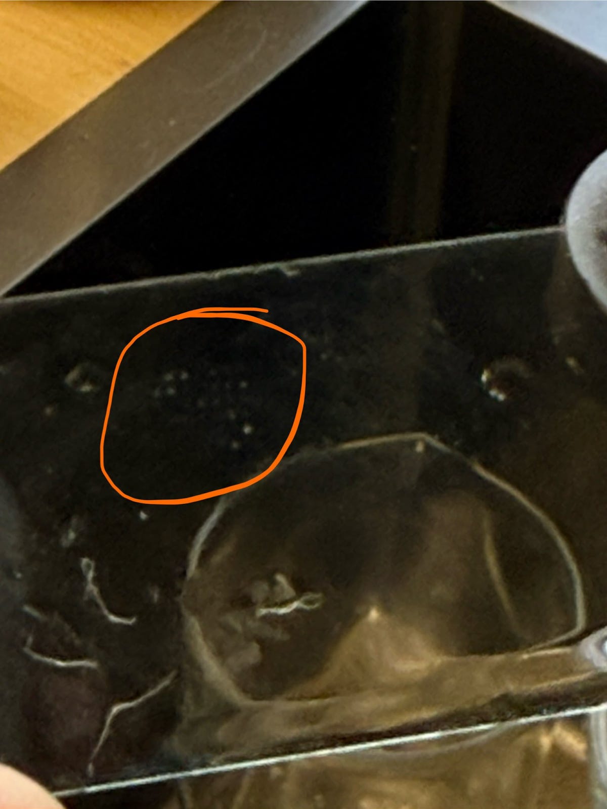
The biggest challenge so far is creating continuously conducting traces. In theory, we could just make the traces thicker. We increased the widths in SVGs (a set of lines defined in the XML format).1 However, in practice for SVGs, the laser software treats all lines as infinitely thin. We then tried the JPGs, which are bitmaps, however, the microchanges from 0.2 mm to 0.3 mm in the JPG was pathetically insignificant, leading to a fuzzy, shorted circuited image. A lazy hack we found was just to duplicating the traces three times in the laser software from xtool. Additionally, we varied the scan rate (+/- 20 mm/s) and lines per cm (max at 200, min at 50) and set the laser scanning to be monodirectional.
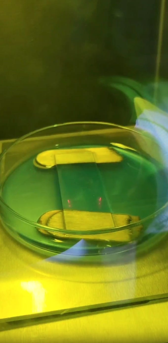
Examining the conductivity of trails:
The triple-layered electrode version was consistently conductive. The next step would be to test it in saline and compare to the standard Utah array.
Aluminum vapour deposition
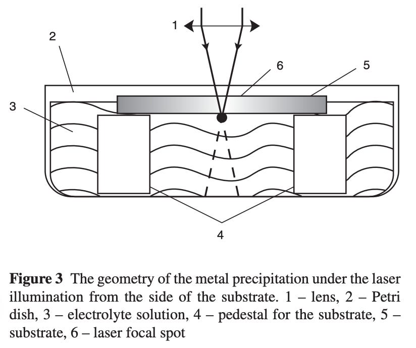
While trying the above, we accidentally turned the power too high, causing metal to be directly deposited onto glass! It certainly didn’t look like graphene. So we peeled off the tape, put the glass slide into the laser chamber and turned the laser on again. This was indeed the vapour from the underlying sheet of aluminum. Here, we used a diode-pumped solid state laser (DPSS) of 1064 nm (see physical vapour deposition).
Copper metalization
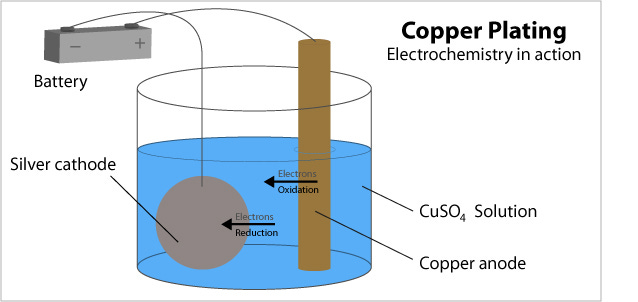
A focused laser beam is directed at the copper solution, causing heated surfaces at particular points and unheated surfaces. This creates a voltage difference like a battery. The heated area gains copper under the plate.
This is analogous to the traditional electroplating process where an object (cathode) is coated with a thin layer of metal. The cathode connected to negative terminal of the battery and the metal to be deposited the opposite. When DC current is applied, metal atoms at the anode lose electrons, swim through the solution toward the cathode. The metal atoms here are positive and are attracted by the cathode’s negativity. Simplified copper reaction: Cu²⁺ + 2 e⁻ → Cu(s).
Here is what the setup looked like:
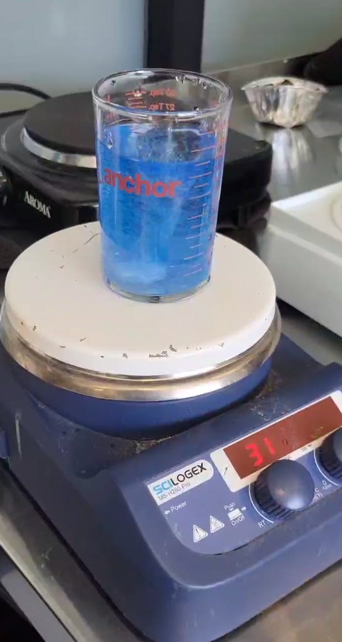
Preparing the electroplating solution:
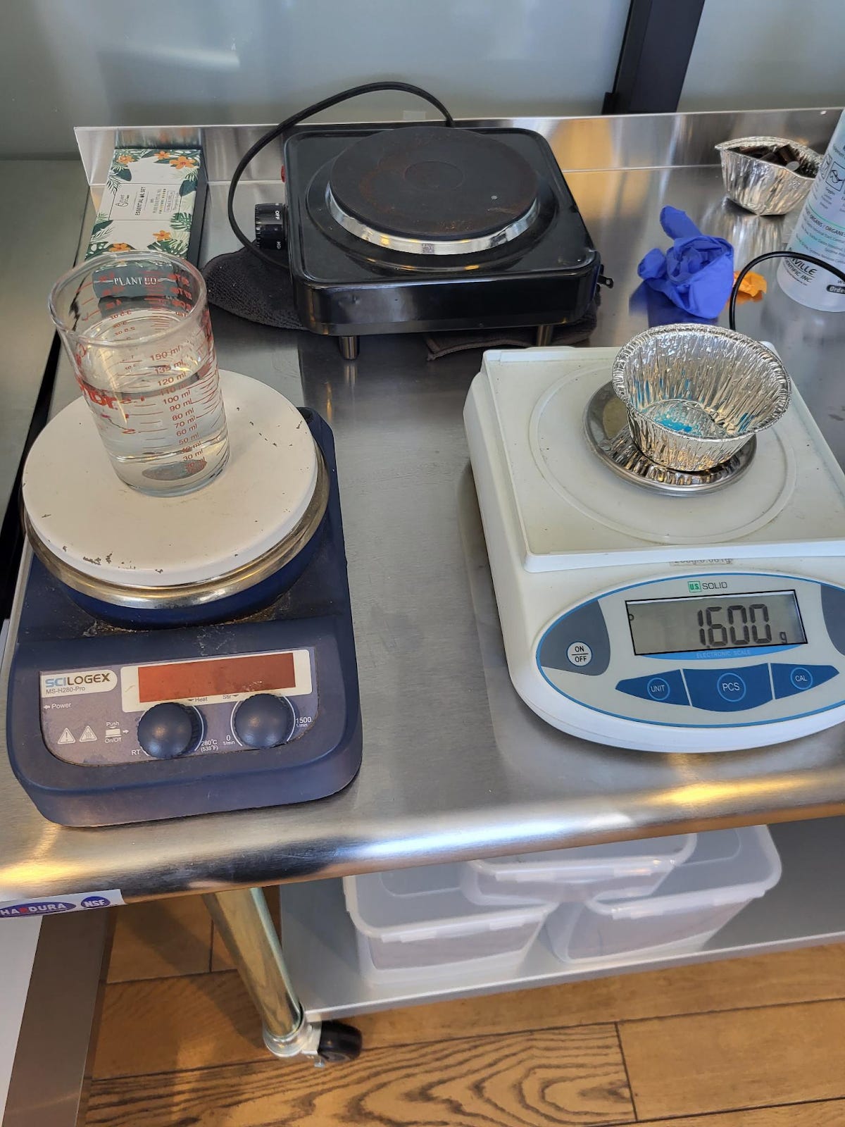
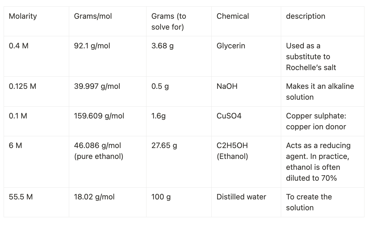
Add water first, and then go from least reactive to most. Make sure to add distilled water, followed by alcohol, glycerin, NaOH and then CuSO4. We placed the solvent on a hot plate, with a magnetic rod for stirring.
The biggest challenge here was when the equipment behaves inconsistently, especially for the scale: We became suspicious when the 100 mL of water weighed 125 grams! The 2nd replication, the copper solution instantly precipitated to copper hydroxide, a cloudy, turquoise colour. Quickly, we thought of several other solutions such as switching power supplies, using different scales, but there weren’t matching power supplies of 9V for any other scale! So, I poured in some ethanol (1 mL of ethanol was 0.789 grams) to see how much the scale was off by, which was roughly the same offset (29.5875 grams). From then on, we performed everything according to the scale’s offset mass (1.25x).
PEDOT:PSS traces
What if we want some transparent MEAs? Researchers may use red and green fluorescent proteins in their living neurons which includes filtering colours. If someone were to use mCherry red fluorescent proteins + if the filter is narrow, the tape would appear dark and cover up everything else.
Here are some materials to use (loosely inspired by this paper)
Indium tin oxide coated borosilicate glass - The transparent material
Brush-on negative insulator (1002F epoxy) - To cover the non-conductive regions
PEDOT:PSS (PH1000 + 5 % DMSO or ethylene-glycol) - Making the surface biocompatible, although ITO is already safe.
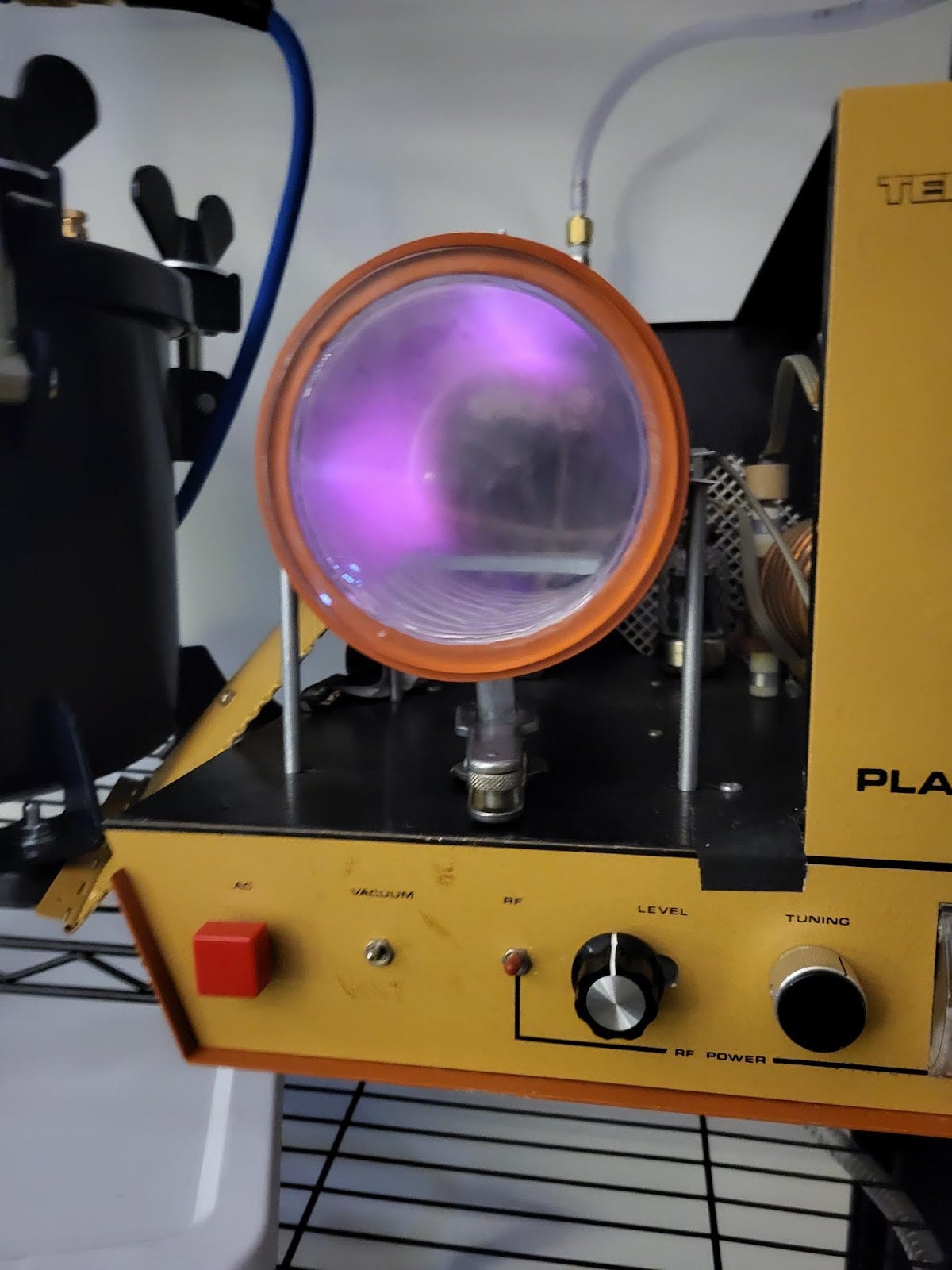
This method is in-progress! We could use the plasma engine to increase the surface energy of glass.
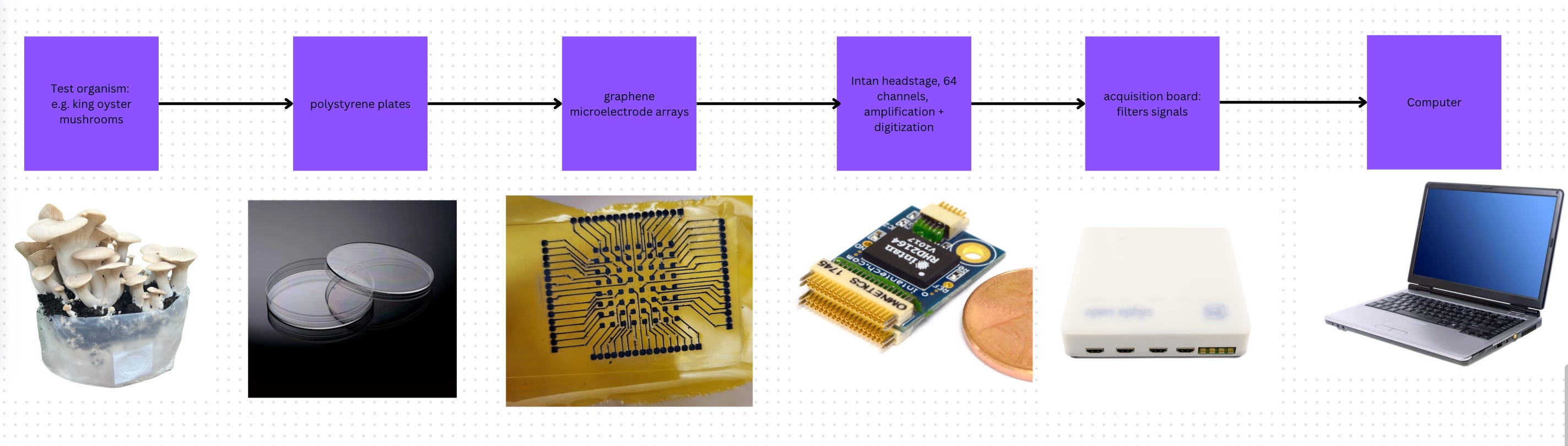
So! Once we have the MEA, we would just need the below systems for neural signal processing! The cost is estimated to be $3k.
Collaborators: Eigenlucy, Morgan Hough, Lucas Mair, James Mavo.
SVG stands for scalable vector graphics, so it’s easy to rescale them in any text editor or graphics software. Inkscape is one of my favourite drawing softwares.
this is great - are you doing this by yourself or within a lab?